
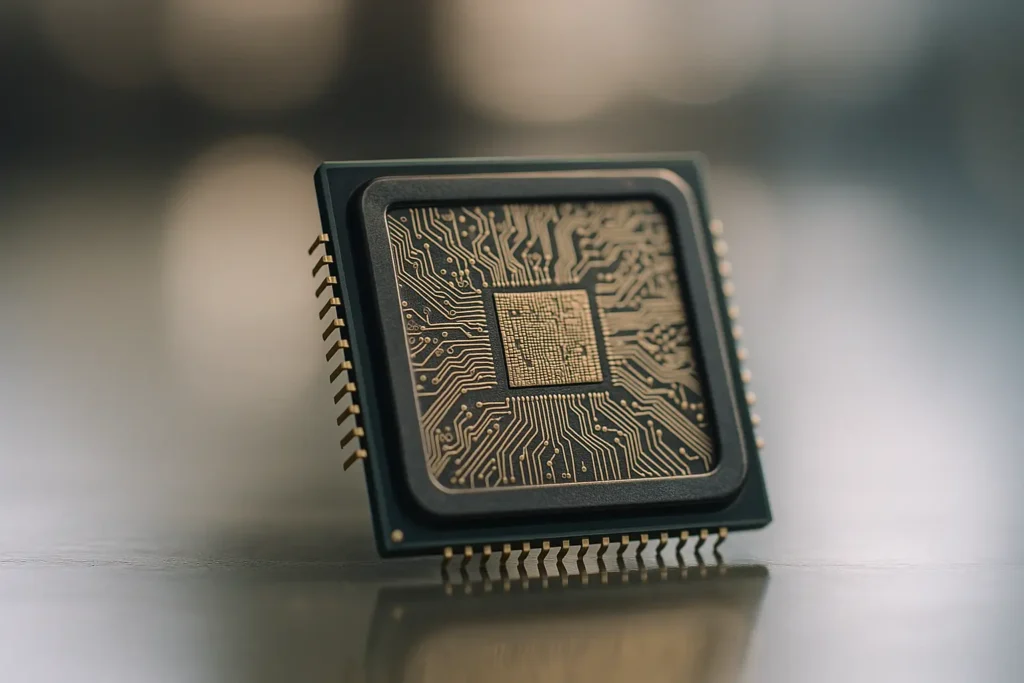
The processor in the phone on your desk spent longer in production than a car spends being designed for a facelift. Industry association figures put the journey from customer order to finished, packaged chip at up to twenty-six weeks, most of it inside a building the chip’s eventual owner will never see. That lead time explains more about shortages, pricing and geopolitics than any diagram of a transistor ever will.
Key takeaways
- Wafer fabrication alone runs about eleven to thirteen weeks, longer on leading-edge nodes.
- A single High-NA extreme ultraviolet lithography system costs in the region of 400 million dollars.
- TSMC’s 2nm class node entered volume production in the fourth quarter of 2025, priced at roughly 30,000 dollars per wafer.
- Assembly, test and packaging add around six weeks and are concentrated in a handful of countries.
The wafer, and why purity is the hard part
Silicon is the second most abundant element in the earth’s crust, which is why the sand-to-chip framing is so popular and so misleading. Abundance was never the constraint. Purity is. Metallurgical silicon is refined until impurities are measured in parts per billion, then melted and slowly pulled into a single cylindrical crystal with a consistent atomic lattice throughout. Get one dislocation in that lattice and the dies around it are scrap.
The crystal is sliced into wafers, most commonly 300 mm across, then lapped, etched and polished until the surface is flat to within a few nanometres. That preparation alone can take several weeks, and it happens before a single transistor exists. The wafer arriving at a fab is already an expensive, highly engineered object.
Printing features smaller than the wavelength that draws them
The patterning stage is where the money is. Extreme ultraviolet lithography uses light at 13.5 nanometres, produced by hitting droplets of molten tin with a laser, reflected through mirror optics because no lens material transmits at that wavelength. The current generation, ASML’s High-NA systems, cost around 400 million dollars each. ASML shipped its first EXE:5200 production scanner in 2025, with Intel as the lead adopter for its 14A node, while TSMC has said it will push conventional EUV with multi-patterning on its first A14 generation rather than switch immediately.
Lithography is only one step among hundreds. Each layer is deposited, patterned, etched and cleaned, then measured, and a leading-edge chip has dozens of such layers stacked in precise alignment. TSMC’s N2 generation, which entered volume production in the fourth quarter of 2025, is also its first to use gate-all-around transistors, where the gate wraps the channel on every side to control leakage that fin structures could no longer contain.
| Phase | What happens | Indicative duration |
|---|---|---|
| Substrate preparation | Purification, crystal growth, slicing, polishing | Two to six weeks |
| Wafer fabrication | Hundreds of deposition, lithography and etch steps | Eleven to thirteen weeks, longer at the leading edge |
| Assembly, test and packaging | Dicing, bonding, encapsulation, electrical test | Around six weeks |
| Order to delivery, total | All of the above plus queueing between steps | Up to twenty-six weeks |
Note the gap between the sum of the phases and the total. Lots spend a substantial share of their time waiting for a tool rather than being processed, which is why fabs are scheduled with the obsessiveness usually associated with airline operations.
The back end nobody photographs
Once the wafer is finished it is tested, then diced into individual dies, and the good ones are packaged. Packaging used to be the dull final step. It is now a competitive frontier, because stacking memory beside or on top of logic in a single package delivers gains that shrinking transistors alone no longer provides at an acceptable cost.
Geography matters here. Fabrication and advanced packaging capacity sit in a small number of locations, and the materials feeding them do too, which is the same structural dependency we described when looking at why rare earths returned to the industrial agenda. A chip crosses several borders before it reaches an assembly line, and every one of those crossings is a policy variable rather than a logistics detail.
Questions worth asking about all this
Does a smaller node number mean a faster phone? Not directly. Node names stopped describing a physical dimension years ago and now function as generation labels. What a new node reliably offers is better performance per watt, which on a phone shows up as battery life more often than as raw speed.
Why can’t a fab simply add a shift when demand spikes? Because the constraint is tool capacity and cycle time, not labour hours. Adding output means adding equipment with long lead times, and even then the first wafers are twelve weeks away.
Are 30,000 dollar wafers passed on to consumers? Partly, and diluted heavily. A 300 mm wafer yields a large number of dies, so the per-chip silicon cost is a modest share of a handset’s bill of materials. The bigger commercial effect is on which customers can afford to design for a leading-edge node at all.
What actually caused the shortages of the early 2020s? A demand shift combined with lead times measured in months, in a supply chain with almost no buffer stock. When ordering and receiving are separated by half a year, a forecasting error becomes a shortage before anyone can correct it.
What this means for the object in your hand
The chip in a current smartphone represents several months of continuous, sequential work in facilities that cost tens of billions to build, using a handful of machines that only one company in the world makes. That concentration is the real story, more than the transistor count on the spec sheet.
It also sets a useful expectation. Improvements arrive on a cadence set by capital equipment and construction schedules, not by software release cycles. When a generation of devices feels like an incremental step, the explanation is usually sitting in a cleanroom two years upstream, waiting for a tool that has not shipped yet.
Following where all this silicon ends up?
The largest single buyer of leading-edge capacity today is not the smartphone industry.
Sources: Semiconductor Industry Association, published guidance on semiconductor manufacturing lead times, including up to twenty-six weeks from order to delivery and roughly six weeks for assembly, test and packaging; TSMC disclosures and trade reporting on N2 volume production from the fourth quarter of 2025, gate-all-around transistors and wafer pricing of approximately 30,000 dollars; ASML statements on the shipment of its first EXE:5200 High-NA extreme ultraviolet system and Intel’s adoption for the 14A node. Durations are industry-typical ranges and vary by product, node and fab loading. Updated August 2026.